This sequential device loads the data present on its inputs and then moves or “shifts” it to its output once every clock cycle, hence the name “ shift register”. A shift register basically consists of several single bit “D-Type Data Latches”, one for each data bit, connected together in a serial type daisy-chain arrangement so that the output from one data latch becomes the input of the next latch and so on. Data bits may be fed in or out of a shift register serially, that is one after the other from either the left or the right direction, or all together at the same time in a parallel configuration. The number of individual data latches required to make up a single Shift Register device is usually determined by the number of bits to be stored. Shift Registers are commonly used inside calculators or computers to store data such as two binary numbers before they are added together, or to convert the data from either a serial to parallel or parallel to serial format.
The individual data latches that make up a single shift register are all driven by a common clock ( Clk ) signal making them synchronous devices. Shift register IC’s are generally provided with a clear or reset connection so that they can be “SET” or “RESET” as required. Generally, shift registers operate in one of four different modes with the basic movement of data through a shift register such as: • Serial-in to Serial-out (SISO): The register is loaded with serial data,one bit at a time, and shifted serially out of the register, one bit at a time in either a left or right direction under clock control. • Serial-in to Parallel-out (SIPO): The register is loaded with serial data, one bit at a time, with the stored data being available at the output in parallel form. • Parallel-in to Serial-out (PISO): The parallel data is loaded into the register simultaneously and is shifted out of the register serially one bit at a time under clock control. • Parallel-in to Parallel-out (PIPO): The parallel data is loaded simultaneously into the register, and transferred together to their respective outputs by the same clock pulse.
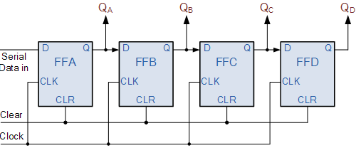
The effect of data movement from left to right through a shift register can be presented graphically as: Fig.1 Serial-in to Serial-out (SISO) Shift Register Let all the flip-flop be initially in the reset condition i.e. Q A = Q B = Q C = Q D = 0. We enter a four bit binary number 1 1 1 1 into the register. This number should be applied to D in bit, with the LSB bit applied first. The D input of FFA i.e. D A is connected to serial data input D in. Output of FFA i.e.

How to design a 4-bit Serial In Parallel Out shift register (SIPO)? Then we know that we have a serial output so let’s connect the output of the last flip-flop to the output pin. The first flip-flop also does not need a serial input because there is no preceding flip-flop. Parallel in, parallel out, serial input.
To share this torrent use the code below and insert it into comments, status messages, forum posts or your signature. Torrent: Vag-Com 409 1 + Crack [EDAXAK]. Install Vag-com Step 2-Run Vag-com 409.0 Crack it will ask for the location where you installed vagcom. And will install 3 files. Named D1 D2 D3. Step 3-Open the Vag-com Directory in program files. And Create a new folder named C now copy past the 3 files named D1 D2 D3 into the folder called C. Step 4-Open Notepad and copy past this into it. Vag com 409 crack torrent.